- 您现在的位置:买卖IC网 > Sheet目录2002 > LTC1096IN8#PBF (Linear Technology)IC A/D CONV 8BIT SRL IN/OUT 8DIP
LTC1096/LTC1096L
LTC1098/LTC1098L
18
10968fc
APPLICATIONS INFORMATION
Multiplexer (MUX) Address
The bits of the input word following the START bit assign
the MUX conguration for the requested conversion. For
a given channel selection, the converter will measure the
voltage between the two channels indicated by the “+”
and “–” signs in the selected row of the followintg tables.
In single-ended mode, all input channels are measured
with respect to GND.
MSB-First/LSB-First (MSBF)
The output data of the LTC1098(L) is programmed for
MSB-rst or LSB-rst sequence using the MSBF bit.
When the MSBF bit is a logical one, data will appear on
the DOUT line in MSB-rst format. Logical zeros will be
lled in indenitely following the last data bit. When the
MSBF bit is a logical zero, LSB-rst data will follow the
normal MSB-rst data on the DOUT line. (see Operating
Sequence)
MUX ADDRESS
SGL/DIFF
1
0
ODD/SIGN
0
1
0
1
CHANNEL #
0
+
–
1
+
–
+
GND
–
SINGLE-ENDED MUX MODE
DIFFERENTIAL MUX MODE
10968 AI03
OUTPUT CODE
1 1 1 1 1 1 1 1
1 1 1 1 1 1 1 0
0 0 0 0 0 0 0 1
0 0 0 0 0 0 0 0
INPUT VOLTAGE
VREF – 1LSB
VREF – 2LSB
1LSB
0V
INPUT VOLTAGE
(VREF = 5.000V)
4.9805V
4.9609V
0.0195V
0V
10968 AI05
0V
1LSB
V
REF
–2LSB
V
REF
–1LSB
V
REF
VIN
0 0 0 0 0 0 0 1
0 0 0 0 0 0 0 0
1 1 1 1 1 1 1 1
1 1 1 1 1 1 1 0
10968 AI04
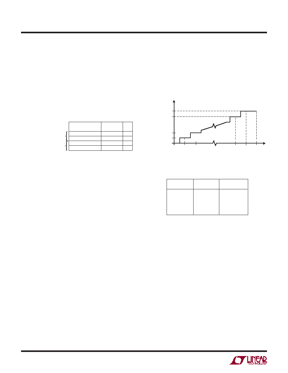
Unipolar Transfer Curve
The LTC1096(L)/LTC1098(L) are permanently congured
for unipolar only. The input span and code assignment for
this conversion type are shown in the following gures
for a 5V reference.
Unipolar Transfer Curve
LTC1098(L) Channel Selection
Unipolar Output Code
Operation with DIN and DOUT Tied Together
The LTC1098(L) can be operated with DIN and DOUT tied
together. This eliminates one of the lines required to com-
municate to the microprocessor (MPU). Data is transmit-
ted in both directions on a single wire. The processor pin
connected to this data line should be congurable as either
an input or an output. The LTC1098(L) will take control of
发布紧急采购,3分钟左右您将得到回复。
相关PDF资料
LTC1099ACN#PBF
IC A/D CONV 8BIT HI-SPEED 20-DIP
LTC1197IMS8#PBF
IC ADC 10BIT 500KHZ SHTDWN 8MSOP
LTC1198-1BCS8#PBF
IC ADC 8BIT 750KHZ SAMPL 8-SOIC
LTC1257IS8#TRPBF
IC D/A CONV 12BIT VOLT OUT 8SOIC
LTC1276ACN#PBF
IC A/D CONV 12BIT SAMPLING 24DIP
LTC1278-4IN#PBF
IC A/DCONV SAMPLNG W/SHTDN 24DIP
LTC1279CG#TRPBF
IC A/DCONV SAMPLNG W/SHTDN24SSOP
LTC1282ACN#PBF
IC A/D CONV SAMPLING W/REF 24DIP
相关代理商/技术参数
LTC1096IN8-PBF
制造商:LINER 制造商全称:Linear Technology 功能描述:Micropower Sampling 8-Bit Serial I/O A/D Converters
LTC1096IN8-TR
制造商:LINER 制造商全称:Linear Technology 功能描述:Micropower Sampling 8-Bit Serial I/O A/D Converters
LTC1096IN8-TRPBF
制造商:LINER 制造商全称:Linear Technology 功能描述:Micropower Sampling 8-Bit Serial I/O A/D Converters
LTC1096IS8
功能描述:IC A/D CONV 8BIT SRL IN/OUT8SOIC RoHS:否 类别:集成电路 (IC) >> 数据采集 - 模数转换器 系列:- 标准包装:2,500 系列:- 位数:16 采样率(每秒):15 数据接口:MICROWIRE?,串行,SPI? 转换器数目:1 功率耗散(最大):480µW 电压电源:单电源 工作温度:-40°C ~ 85°C 安装类型:表面贴装 封装/外壳:38-WFQFN 裸露焊盘 供应商设备封装:38-QFN(5x7) 包装:带卷 (TR) 输入数目和类型:16 个单端,双极;8 个差分,双极 配用:DC1011A-C-ND - BOARD DELTA SIGMA ADC LTC2494
LTC1096IS8#PBF
功能描述:IC A/D CONV 8BIT SRL IN/OUT8SOIC RoHS:是 类别:集成电路 (IC) >> 数据采集 - 模数转换器 系列:- 标准包装:2,500 系列:- 位数:16 采样率(每秒):15 数据接口:MICROWIRE?,串行,SPI? 转换器数目:1 功率耗散(最大):480µW 电压电源:单电源 工作温度:-40°C ~ 85°C 安装类型:表面贴装 封装/外壳:38-WFQFN 裸露焊盘 供应商设备封装:38-QFN(5x7) 包装:带卷 (TR) 输入数目和类型:16 个单端,双极;8 个差分,双极 配用:DC1011A-C-ND - BOARD DELTA SIGMA ADC LTC2494
LTC1096IS8#TR
功能描述:IC ADC 8BIT SERIAL I/O 5V 8SOIC RoHS:否 类别:集成电路 (IC) >> 数据采集 - 模数转换器 系列:- 标准包装:2,500 系列:- 位数:16 采样率(每秒):15 数据接口:MICROWIRE?,串行,SPI? 转换器数目:1 功率耗散(最大):480µW 电压电源:单电源 工作温度:-40°C ~ 85°C 安装类型:表面贴装 封装/外壳:38-WFQFN 裸露焊盘 供应商设备封装:38-QFN(5x7) 包装:带卷 (TR) 输入数目和类型:16 个单端,双极;8 个差分,双极 配用:DC1011A-C-ND - BOARD DELTA SIGMA ADC LTC2494
LTC1096IS8#TRPBF
功能描述:IC A/D CONV 8BIT SRL IN/OUT8SOIC RoHS:是 类别:集成电路 (IC) >> 数据采集 - 模数转换器 系列:- 标准包装:2,500 系列:- 位数:16 采样率(每秒):15 数据接口:MICROWIRE?,串行,SPI? 转换器数目:1 功率耗散(最大):480µW 电压电源:单电源 工作温度:-40°C ~ 85°C 安装类型:表面贴装 封装/外壳:38-WFQFN 裸露焊盘 供应商设备封装:38-QFN(5x7) 包装:带卷 (TR) 输入数目和类型:16 个单端,双极;8 个差分,双极 配用:DC1011A-C-ND - BOARD DELTA SIGMA ADC LTC2494
LTC1096IS8-PBF
制造商:LINER 制造商全称:Linear Technology 功能描述:Micropower Sampling 8-Bit Serial I/O A/D Converters